Introducing 74HC193 Simulation to LTspice

April 21st, 2008

Ron Fredericks writes: I have completed the design and test of a new component for LTspice/SwitchCAD III circuit simulation and schematic capture. In a previous post I discussed my interest in the 74193 presettable synchronous 4-bit binary up/down counter IC for a digital volume control circuit I am building. The circuit simulation described below focuses on how to simulate the 74HC193 IC, but timing and voltage parameters built into this design allow a designer to easily simulate other variants of this IC from high speed Si-gate CMOS HC and HCT devices to low power Schottky TTL devices.

All circuits related to this 74HC193 simulation are available here>

The 74HC193 Component

See figure 1 below for a screen shot of the completed design. The circuit was built from the digital gates in the component library supplied with the original Linear Technology’s free LTspice tool.

74HC193 Circuit and Related Components
Figure 1 – 74HC193 Circuit and Related Components

View larger image>

To keep the design looking like the original data sheet logic diagram, as published by companies that include NXP Semiconductors and Texas Instruments, a custom “T notS-R FlipFlop” subcomponent and corresponding assembly file was first created. This subcomponent was reused 4 times in the main IC logic diagram. An assembly file called 74hc193.asy was also created. It includes all pins used on the commercial IC except ground and Vcc. The IC’s internal power supply is not simulated by the Linear Technologies’ gates, and so they are not used or required in this design either.

Each gate within the design has a few variables assigned to them so that the IC remains flexible and easy to reuse in new projects:

  • tdgate right 
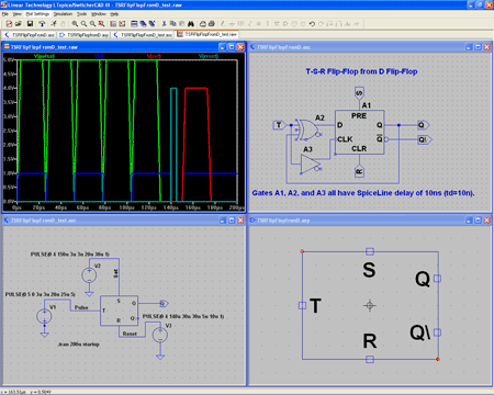
td (propagation time delay assigned to each gate)
  • tdgate2 right td (propagation time delay assigned to the D FlipFlop)
  • tripdtgate right tripdt (td’s accuracy band assigned to each gate including the D FlipFlop)
  • vhighgate right logical high value for each gate and D FlipFlop
  • vlowgate right logical low value for each gate and D FlipFlop

These variables can be assigned their corresponding time and voltage values using a .param statement placed in the main circuit. These values are then within scope for automatic reuse by the 74HC193 component and flipflop subcomponent simulations. Below is an example of how parameter assignment can be made (as used in the test circuit described next):

.param tdgate=10n tdgate2=3*tdgate tripdtgate=1n vhighgate=5v vlowgate=0v

Read the rest of this entry »

Technorati Tags: , , , , , , , , , , , , , , ,

New Gate Design Using LTspice/SwitcherCAD III

April 15th, 2008

Ron Fredericks writes: recently I discovered that I was going to have to create my own IC component and symbol for my on-going digital volume control circuit simulation. My first step was to check in with the LTspice forum on yahoo groups. On the forum I requested any previous design for the IC I needed. I also asked the group’s readership if they thought it was correct to build a new IC from existing low level digital gates – gates that are already supplied with the LTspice distribution by Linear Technologies.

Well, I did not find a previous inventor for my IC simulation, but I did get confirmation that the gate build-up was a common strategy. And, this same forum engineer supplied me with a copy of an IC simulation of his own – one very similar to my IC requirement – he supplied a symbol and sample test bed to accelerate my learning curve. Here is a link to my support dialog.

I would like to thank Helmut Sennewald for his time and excellent service to the LTspice yahoo forum. It is his effort and many others who make this forum such a valuable community resource. This forum in turn, has made the LTspice/SwitcherCAD III circuit capture and spice tool a viable design tool for many embedded component users and EE designers.

Introducing the T S-R Flip-Flop

To build my new IC, I had to build a new digital logic block. This component is a Toggle Flip-Flop with Set and Reset functions added. In this blog post I introduce my readers to this new component and share the simulation circuit for others to use and learn from.

See the figure below for an initial design of the T S-R Flip-Flop, including a truth table in the form of a waveform diagram, the circuit, a pulse detector sub-circuit and their related assemblies. This circuit is just an initial design because it uses an S-R Flip-Flop and a simple pulse detector sub-circuit for its clock.

T S-R Flip-Flop and releated sub-circuits and assemblies

View larger image>

Final Design for the T S-R Flip-Flop

This section of my post is an update, thanks to a review by Helmut Sennewald. See figure below for my final design of the Toggle S-R Flip-Flop. This design overcomes two problems in my initial design, both resolved by starting with the D Flip-Flop with its built-in clock. The reuse of this more full-featured LT supplied component in my design eliminated the home-brew pulse maker sub-circuit. And in so doing, the slower S-R Flip-Flop. Slower because I had to set the SpiceLine time delay to a minimum of 20 nanoseconds (or td >= 2x the gate time delay) to support the simulation of my simple pulse maker sub-circuit. The D Flip-Flop has an internal clock so I could eliminate the pulse maker sub-circuit. End result: one less sub-circuit and faster Flip-Flop simulation using a time delay set to a minimum of 10 nanoseconds (or td >= 1x the gate time delay).

T S-R Flip-Flop (final design)

View larger image>

Download

To test my knowledge of digital design using the LTspice tool, I created a number of similar flip-flop components which are included in the download:

  1. S-R Flip-Flop test circuit
  2. S-R Flip-Flop with Enable gate and test circuit
  3. S-R Flip-Flop with rising edge clock and test circuit
  4. J-K Flip-Flop with rising edge clock and test circuit
  5. D Flip-Flop with Enable gate and test circuit
  6. T S-R Flip-Flop from S-R Flip-Flop and test circuit (initial design)
  7. Rising Edge Pulse Detector (not high performance design)
  8. T S-R Flip-Flop from D Flip-Flop and test circuit (final design)

Download the components listed above for your LTspice designs all in one zipped directory.

Technorati Tags: , , , , , , ,

Simulating the 555 IC with LTspice

March 26th, 2008

Ron Fredericks writes: I was designing a simple CMOS timer circuit around a 555 chip this evening. It might be the heart beat for a new digital volume control I have been thinking about. Normally I look for my breadboard and parts box but this time I thought I would try out Linear Technologies LTspice/SwitcherCAD III workbench instead.

SwCAD III First Time Use

The tool is free and comes with a lot of support. I downloaded the software and installed it very easily on my Windows XP PC. It includes a graphical schematic design tool with lots of ready made simulated components, including an NE555 for my initial project. Designing the circuit with the built-in CAD tool works very intuitively. While the LTspice simulation took a bit of head scratching before it worked for me.

I was able to configure and run the simulation using the drop down tools menu and the little “running person” icon on the tool bar. But all I could get out of the simulation was a black screen with voltage and timing ticks along the left and bottom edges. So my first problem was in realizing that the visual display would remain black and traceless until I put the mouse cursor over a wire then click. When the little instrument probe showed up as my mouse icon, I realized what was going on here. With the mouse click, waveform tracings would appear in the black panel.

My second problem was that the circuit would not oscillate. Not good for an oscillator design. First, I forgot to connect the 555’s threshold + trigger pins to the R2-C2 node using the wire tool. But still no oscillation, just flat line traces were observed. Now I already know that getting circuits to oscillate follows Murphy’s Laws: Oscillators remain stable, Amplifies and Buffers oscillate, whenever possible. I found a note on the Old School Hacker blog with a fine solution. You must simulate the circuit with a power supply starting from 0 volts rather than just have an instant on Vcc power supply.

In hind sight dah, its the initial transient response from the circuit’s components that kicks the oscillator into oscillating.

After a little practice I improved the schematic diagram with the use of named nodes and seperation of the temporary load resistors R3 and R load from the more permanent circuit components. The load resistors are just place holders for a real load to be added to the circuit schematic next. Look for my next blog post on this subject.

Finally, I used the cursor measurement facility built into the LTspice window (trace window). With this feature, I was able to make “real” measurements on the waveform for frequency and duty cycle.

Circuit

Here is what I was able to generate using the LTspice/SwitcherCAD III tool:

LTspice/SwitcherCAD III circuit diagram and waveforms

View larger image>
Download 555 Astable Flip-Flop Schematic Circuit Diagram>

Referring to the figure above:
   Green Trace -> Output (IC 555 pin 3)
   Blue Trace -> Trigger / Threshold (IC 555 pins 2 & 6)
   Red Trace -> Discharge (IC 555 pin 7)

The Astable Multivibrator

The circuit shown above will trigger itself and free run as a multivibrator. The capacitor C2 charges through resistors R1 and R2 yet discharges through R2 only. Thus, the duty cycle (D) may be precisely set by the ratio of these two resistors. The capacitor charges and discharges between 1/3 Vcc and 2/3 Vcc. But the initial pulse charges C2 starting from 0 Vcc and so this first pulse duty cycle is unique. Since the charge rate and the threshold levels are directly proportional to the supply voltage Vcc, the frequency of oscillation (f) is independent of the supply voltage.

Frequency Calculation Duty Cycle Calculation
   
f = 1.38/{(R_1 + 2R_2)C_2} D = {tau}/T = {R_1 + R_2}/{R_1 + 2R_2}
   
1.7 hertz=1.38*10^3/{(150 + 2*332) ohm farads} 0.59~={150 + 332}/{150 + 2*332}
   
Measured = 1.8 hertz Measured = 0.60
   
Where:
    f 
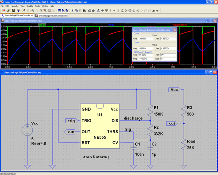
is frequency in hertz
    C is capacitance in farads
    R is resistance in ohms
Where:
    D is duty cycle
    tau is non-zero output duration
    T is the period of the output
    R is resistance
   

Reference

Technorati Tags: , , , , , ,

WordPress Math Publisher Plugin Support

March 24th, 2008

Ron Fredericks writes: This is just a short post to point my readers to a new mathematics publishing plugin available from ECI’s Blog Center. This plugin offers a simple alternative to the more standard approaches: XML’s MathML and Math into LaTeX.

WordPress Math Publisher plugin home page
www.embeddedcomponents.com/blogs/wordpress/wpmathpub/

Usage

An example of how it can be used is your blog posts:

WordPress code…
[pmath size=16](a^2+b^2)=a^2+2ab+b^2[/pmath]
where:
[pmath size=12]~a[/pmath] is defined as a
[pmath size=12]~b[/pmath] is defined as b

Results in:

(a^2+b^2)=a^2+2ab+b^2

where:
~a is defined as a
~b is defined as b

References:
  Pascal Brachet’s phpmathpublisher
    Home: www.xm1math.net/phpmathpublisher/
    Usage: www.xm1math.net/phpmathpublisher/doc/help.html
  Matteo Bertini’s WordPress plugin called PHP Math Publisher
    www.slug.it/naufraghi/programmazione-web/wpmathpublisher
  Randy Morrow’s WordPress plugin called Axiom
    wordpress.org/extend/plugins/axiom/#post-2794

Technorati Tags: , , , , , , , , , , ,

How to Leverage the Value of a Board Support Package

November 21st, 2007

Ron Fredericks writes: There are three separate views to what defines an effective Board Support Package (BSP). I believe each of these views is correct as independent descriptions of a BSP. But together these views provide insight into the embedded target from equally important perspectives or engineering disciplines. Read this post to learn more about the essence of embedded systems and how Wind River’s VxWorks BSP architecture has been a critical success factor in comparison to many other real-time embedded operating system executives and kernels available today.

I chose to discuss Wind River’s VxWorks BSP because of my familiarity with their product line, my understanding of their BSP as a competitive product compared to other real-time kernels, and because of my industry accomplishments working with Wind River’s BSPs:

  • Ron Fredericks wins Wind River’s prestigious Navigation Award for designing, launching, and marketing the first online interactive social network for BSP’s. more>
  • Ron Fredericks wins Aiysis’ Million Dollar Club Award for nurturing a Wind River partnership between VxWorks and Aiysis DriveWay BSP tool kit that generated over one million in annual sales. more>
  • Ron Fredericks co-author’s an article with Xilinx on How to Design Field Upgradable Systems based on FPGA Internet connectivity with VxWorks BSP’s. more>
  • Ron Fredericks produces an online video: How to Prototype a Device Driver [or BSP] in Less Than – Wow! – 5 Minutes for a Freescale application processor / communications co-processor System on Chip (SoC). more>

A similar high level discussion can not be made for most embedded Windows or embedded Linux BSP’s today. This is because the BSP for these monolithic kernels are not as modular as a real-time executive kernel such as VxWorks. Indeed other real-time kernel vendors can and do take advantage of the BSP too. But, the VxWorks BSP just took more advantage of this natural separation between board support and kernel tasks earlier in the marketplace and has been an advantage for its customers as a result ever since.

Target Board with BSP connected to a host workstation
Figure 1 – Embedded device with BSP connected to a host workstation

As shown in Figure 1, most BSP’s today, even those for embedded Windows and embedded Linux, do have a robust set of boot options. In many cases a BSP can be used on its own to network attach to a shared file system where the full operating system and application can be loaded. In this way, a device under development need not be the device where development takes place. The BSP in this case forms the basis for a cross-platform development environment – a big plus for developers of embedded systems. Developers often expect cross-platform development to include a BSP with a limited network stack to load new code onto the target hardware during a cold reset. The BSP might use JTAG on-chip run-time control, RS232 serial port, FTP, Bootp, TFTP and RARP, or even a command shell with a full network stack, as the boot loading protocol. But what ever host to target connectivity is used, cross-development allows a high end workstation to be used for time-saving development along with an easy way to download the resulting compiled relocatable object code or a linked and located image onto an embedded target.

For hardware vendors, the BSP is a very useful partner tool. If a hardware vendor makes a set of boards along with a bus pre-assembled as a subsystem or just a single board computer, the BSP allows its clients to leverage this hardware for software development right away. So a hardware vendor can select major operating systems that meet the needs of its target client base and offer a BSP suitable for these operating systems. Usually the BSP is not a licensed product from the operating system vendor and can be bundled royalty free or under very libral license fee conditions. In this way, the operating system vendor or the open-source community, can partner with this hardware platform as a known reference for direct end products or for development of custom products. The horrible alternative is a slow hardware bring-up using new hardware for the first time to build a unique BSP – a very slow and expensive procedure where few software debug tools are available. JTAG or other N-wire run-control devices can be used with an operating system vendor’s debugger in some cases when a robust BSP is not already available. Silicon vendors and I/O device vendors can leverage this technical marketing strategy too.

I encourage Microsoft and embedded Linux communities to consider improving their BSP strategy to deliver more value from a separate BSP structure too. I also encourage my readers to go ahead and submit comments to this blog post if you know of other vendors with good BSP designs as the marketplace is always changing.

Read the rest of this entry »

ROI as an Effective Communications Tool for Engineers

September 26th, 2007

Abstract

Ron Fredericks writes: Engineers want to build compelling products that meet their project requirements. Corporate executives want to invest in innovative people that build products that, in turn, meet their market’s window; while, both want to stay within budget. Yet both groups may feel overwhelmed with the prospect of expressing the very heart of their inspiration at some critical times during the life of these projects. In today’s post, I try to address this issue from the engineer’s perspective reaching out to the financial decision makers that ultimately control the purse strings of every project.

Table of Contents

Introducing Financial-Speak to Engineers
ROI Example: Embedded Linux
Evaluating Incremental Cash Flows
ROI Example: Simple Project Comparisons Using Net Present Value
ROI Example: Evaluating an Infrastructure Project
ROI Example: The Original Design Manufacturer
References
Errors and Changes Planned for this Blog Post

Introducing Financial-Speak to Engineers

In a previous post I introduced the idea that ethics might be the common framework between this dichotomy in communication between engineers, marketers, and executives. In this post, I suggest that engineers might apply this ethical approach by taking some time out to learn the language of business development from a financial management perspective – a conversational framework suitable for an interdisciplinary team concerned with engineering risk and strategic business value, but expressed using financial definitions.

The term Return On Investment (ROI) can be used for all three disciplines: engineering, marketing, and finance. ROI is just vague enough to cover most any discussion an engineer may encounter through-out the life of a project: from the initial decision to fund your project, to evaluating change requests during the design, build, test, and deployment cycle of an ongoing project. Evaluating ROI from a financial perspective is an ethical approach to decision-making because the financial terms I promote for this ethical framework have very precise meanings. So precise in fact, that I too have had to go back and rewrite several sections of this blog post thanks to One Nomad’s Blog comments received in this blog’s first posting.

It was the lack of financial precision embedded within my first draft for this blog post which my guest reader used to convince me of my own mistakes. Yet to be clear, identifying my mistake is also my gain. Effective communication is a process of two or more people sharing ideas…

Learning to converse and plan using financial terms for ROI decision-making can level the playing field between engineers, marketers, and business executives since ROI itself is not a common financial term. Engineers practicing Financial-Speak centered around ROI as the goal, can help reduce many of the common problems related to individuals trying their best to participate in team decision making. This leveling of the playing field – between team members – can also enhance the power of their conversation, leading the way for the much sought after innovations that are in popular demand today.

Consider building a financial model around ROI before presenting your most important technical needs to executives, marketers, and other decision makers. Read on to learn how. Of course ROI from a financial perspective is not the only way to build effective interdisciplinary teams with engineers involved. In a future post I may suggest a corollary to this ethical approach for executives and marketers who would like to reach out to engineers – using Six Sigma, CMMI, and emerging techniques developed by Dr. Thomas J. Buckholtz as useful processes seeped in ROI terminology.

Figure 1: Net Present Value Equation

NPV(CF_k, R, IV) := IV+delim{[}{sum{k=1}{N}{CF_k/(1+R/100)^k}}{]}

Where:
NPV is the Net Present Value function, in dollars
CF is a project’s Cash Flow, in dollars
R is the hurdle Rate, in percent per period
IV is the Initial Investment (a negative number), in dollars
And:
k is the cash flow’s time increment, or period
N is the total number of cash flow periods for k
Time increment for CF and R might be in years, quarters, or months, for example

ROI Example: NPV’s Effect on Embedded Linux

The equation in Figure 1 forms the heart of my “ethics in engineering” proposal. Namely, the sooner a new device gets to market, the sooner a firm can realize new income. New income realized sooner, is much better than income realized later. A finance discussion around NPV would call this time’s negative impact on the value of money. I’m talking about the exponential effect that the prevailing interest rate, R, has in the NPV equation shown in figure 1.

A few years ago several of the leading embedded operating system suppliers used this equation to show that embedded Linux was a poor choice for new embedded device development projects. One such paper published by Dr. Jerry Krasner in 2003, Total Cost of Development, presents the typical argument pretty well. At that time Dr. Krasner and many others may have been right. Now in 2007, times have changed significantly. A recent blog entry on CNET shows the missing element from Dr. Krasner’s report and is a Harold for the embedded industry going forward: Oracle touts Linux deals.

How times have changed…

Because of the significant adoption of Linux in enterprise projects, the total project cost of using embedded Linux has gone down too. Indeed, the migration and reuse of enterprise Windows operating system application programming interfaces (API’s), kernel components, and development tools into embedded device projects was a key part of Dr. Krasner’s report, see link above. Dr. Krasner concluded at the time that embedded Windows CE made the best choice for new projects from a total cost of ownership perspective – just another way of looking at NPV!

Now the ROI benefits behind projects that select embedded Linux follows Dr. Krasner’s logic perfectly. Embedded Linux is now experiencing the same reduced total cost of ownership that only embedded Windows CE enjoyed just a few years ago. The reduced total cost of ownership comes from new and improved tools, components, and API’s that cross over from enterprise projects to the embedded marketplace. There is a significant overlap in Linux kernel updates, components, and tools driven by enterprise projects that are also suitable for use in embedded projects.

The available pool of engineers that know how to work with Linux can now support embedded development projects that use embedded Linux too. The marketing movement around the value and excitement of using Linux may also reduce the cost of taking an embedded device to market. In short: lower upfront costs, more options, more solutions, and faster time to market. Even Dr. Krasner has decided to post an update to his old white paper showing total cost of development to be favorable for embedded Linux projects. Download his updated paper.

None of these enterprise driven benefits exist with respect to the traditional embedded real-time operating system (RTOS). To be clear, there are other benefits to using an RTOS. I discuss one significant benefit to using an RTOS in another post: How to Leverage the Value of a Board Support Package.

Evaluating a Project’s Incremental Cash Flow

NPV is just one example of applying the principle of ROI to making project decisions. NPV falls into the general category of capital budgeting, a process of evaluating proposed investments into new projects. The capital budgeting process is concerned only with incremental cash flows. So the vague concept of ethics can be transformed into a specific financial discussion.

Two financial functions can measure time’s effect on money:

(1) Net Present Value (NPV) expressed as a monetary value,
and

(2) Internal Rate of Return (IRR) expressed as a percentage.

Where:

Net Present Value (NPV) of a capital budgeting project is the dollar amount of change in the value of the firm as a result of undertaking the project [Ref: Financial Management: Principles and Practice P.234]. The mathmatic definition for NPV is:

NPV = IV + Sum[ CF(k) / (1+R)^k ], k ranges from 1 to N

Where:

IV = Initial Investment (a negative number)
CF(k) = cash flow value (project outputs – project inputs) for period k
R = hurdle rate per period
period = a unit of time, typically year, quarter, or month
N = total number of periods for the project

Present Value (PV) is the value today of a future, or expected, cash flow. The mathematic definition for PV is:

PV = Sum[ CF(k) / (1+R)^k ], k ranges from 1 to N

NPV can be expressed in termis of its present value (PV):

NPV = IV + PV

Hurdle Rate is the required rate of return before launching a new project. The hurdle rate must be carefully chosen. It can be expressed as a percent per period. The period is commonly defined as one year, but other convenient time period could be selected such as one quarter, or one month. The same unit of time will need to be associated with cash flow. Other rate terms can be used in addition to, or instead of, hurdle rate: discount rate, cost of capital, or interest rate.

Internal Rate of Return (IRR) is the discount rate at which the
NPV of the project is zero
. [Ref: Financial Management: Principles and Practice P.240]. The mathematic definition for IRR is related to NPV:

0 = IV + Sum[ CF(k) / (1+IRR)^k ], k ranges from 1 to N

NPV and IRR are related to each other:
What follows is a list of relationships between NPV and IRR. Use these relationships after calculating the NPV and IRR for each of the proposed project alternatives.

(1) If NPV(CF,R, IV) = 0,
then the hurdle rate, R = IRR

(2) For any set of cash flows estimated for a prospective project,
there is only one value for NPV.
But, the same project model can result in several IRR values,
where NPV = 0.

(3) If IRR > Hurdle Rate,
then a prospective project may make an acceptable
investment.

(4) If IRR >> Hurdle Rate (i.e. significantly greater than),
then a prospective project may carry too much risk.

(5) The hurdle rate includes both a minimum desired rate
of return for a project, and a threshold representing risk.
(5-a) A typical hurdle rate for an E-Business project
might be 15%.
(5-b) A typical hurdle rate for an embedded systems project
might be 18%.
(5-c) Embedded Components, Inc. is focused on lowering risk
for its members by promoting the re-use of pre-existing
components through its online marketplace
for embedded device manufacturers and their
communities.

(6) In general seek to maximize NPV, not IRR.

(7) Yet, if two projects have NPV curves that cross over each
other,
then the interest R where the curves cross is called
the Crossover Point.
(7-a) If the Crossover Point > IRR,
then accept the project with higher NPV.
(7-b) If the Crossover Point < IRR, then accept the project with higher IRR. (8) An NPV value of zero also means the investment into that project would neither gain nor loose value for the company. Read the rest of this entry »

Technorati Tags: , , , , , , , , , , , , , , ,

An Introduction to the HHP-16K EPROM Emulator

September 9th, 2007

Ron Fredericks writes: The HHP-16K EPROM Emulator allows application code to be read by Hewlett-Packard’s (HP’s) HP-41 calculator. Instead of inserting a small pre-built module into one of the four module bays of the calculator, such as the PPC ROM module discussed in one of my previous blog posts, this unit allows a person to use custom built programs previously stored into EPROMs (Erasable Programmable Read Only Memory devices) using software development tools and an EPROM burner.

Figure 1: HPP-16K Emulator Connected to HP-41 Calculator

HPP-16K EPROM Emulator connected to HP-41 Calculator
Photo by Ron Fredericks using Canon EOS-10D 34mm fluorite lens, UV Filter, 1.5s & f/22 @ ISO 100, on tripod, from Embedded Components’ HP lab collection.

Business Development using EPROM

The HHP-16K represents, a stepping-stone from source code to mass marketing through the use of HP’s commercial software development tools and it’s professional services team. Advertisement and promotion of HP’s professional services to productize HP ROM modules from EPROMs could be found within HP’s own software development tools, and in newsletters – newsletters published by HP and by independent self-assembling developer communities such as national and international versions of the HP Computing Club or HPCC.org. HP’s fee for this service was not trivial, often HP computer clubs would collect donations from 100’s or 1000’s of their members to raise the $20,000 to $60,000 (in 1980’s dollars) to produce these ROM modules for their members – all before the Internet.

This emulator is an example of an important design pattern for modern day software developers forming into ecosystems around mass marketed smart consumer devices!

A typical consumer device in today’s market often has gigabytes of flash memory or other extensions via cellular networks, enterprise networks, or WI-FI Internet access, that behave just like this old 16 kilobyte emulator. With this design pattern – developers can improve the consumer’s experience on popular devices by adding new software applications, middleware, content, and development tools. While at the same time, developers gain significant new business development opportunities for themselves, content providers, software tools vendors, professional services teams, and device manufacturers alike.

Read the rest of this entry »

How to build Dean Lee’s Syntax Highlighter from latest components

May 29th, 2007

Ron Fredericks writes: In my last two posts:

During my research to solve the word wrap problem, I discovered a few more issues leading me to update Dean’s plugin with the latest version of GeSHI (an open-source project: Generic Syntax Highlighter for php. Highlight many languages, including PHP, CSS, HTML, SQL, Java, Assembler, and C for XHTML compliant output) and removal of unused files. I thought other WordPress bloggers might like to take advantage of the latest code too, so I document the steps needed to build a clean plugin with the latest components.

Flow Chart / Swim Lanes Widget
Below is a Flash widget I built to document the steps needed so you can roll your own up-to-date plugin. Follow these steps and you won’t have to be a programmer to get the benefits from the latest versions of these program components. The widget actively links to the latest PHP files and CSS classes:

[flash http://www.embeddedcomponents.com/blogs/wp-content/uploads/2007/05/how2installplugin.swf w=450 h=583]

Read the rest of this entry »

Technorati Tags: , , , , , , , , , , ,

How to Fix Dean Lee’s Source Code Highlight Plugin

May 27th, 2007

Ron Fredericks writes: In my previous post, I discuss Dean Lee’s source code syntax highlighting plugin for WordPress. It delivers all the great features of the GeSHi open-source highlight project for Wordress bloggers.

Yet some source code displayed badly – turning a developer’s nice clean style into a chaotic and messy format. I demonstrated the display problem using a perl sendmail script I plan to discuss in a future blog post. The problem had to do with some kind of whitespace word wrap issue.

I tested various features of CSS and DIV tag attributes created by Dean’s plugin and the GeSHi php code. I am happy to say, I found a simple one-line solution. My solution is in updating Dean’s CSS container class to force white space not to wrap.

Here is my solution:
Add this property to Dean’s “ch_code_container” CSS class:

white-space: nowrap;

Read the rest of this entry »

Technorati Tags: , , , , , , ,

How to Display Source Code Within WordPress

May 25th, 2007

Ron Fredericks writes: I have a problem in common with many software engineers and technical managers – “How can I display source code within my blog?”

See, the problem starts when the source code to be displayed interacts with the blogging software itself and then corrupts the blog’s own loop-and-display engine. Thus, the blog page becomes corrupt or at the very least, becomes mis-formatted and hard to read. Of course it would also be nice to color code a software snippet similar to a source code editor to make the posted source code easier to read.

I tried several techniques during my Internet search for “WordPress source code formatting”. I discovered a common theme – there are source code display and highlighting methods available – in fact too many are available. So the search became a “needle in the haystack” time sink. And the sad fact, most choices have some severe limitations.

But at last, I found Dean Lee’s blog post: Source Code syntax highlighting plugin for WordPress (V1.1)

Dan’s pluglin for WordPress has all the features I was looking for:

  • installs as a simple plugin for WordPress
  • usage within a blog post is easy through the use of the pre tag
  • source code displays in its own container with line numbers for reference
  • a reader should be able to easily select a range of displayed source code and copy it for their own use (without also selecting the displayed line numbers)
  • source code display should not break my WordPress blogging software

Read the rest of this entry »